The IGBT is the core component of the inverter and naturally requires special attention.The most popular and common electronic components used in practical applications are bipolar junction transistors BJTs and MOS tubes.
You can think of an IGBT as a fusion of a BJT and a MOS tube. The IGBT has the input characteristics of a BJT and the output characteristics of a MOS tube. The advantage of an insulated gate bipolar transistor IGBT over a BJT or MOS tube is that it offers greater power gain than a standard bipolar transistor, as well as higher operating voltage and lower MOS tube input losses.
What is IGBT?
IGBT stands for insulated-gate bipolar transistor. Figure (a) shows the symbol of an IGBT. It is a power transistor that combines an input MOS and an output bipolar transistor. Figure (b) shows an example of the IGBT structure. A P region is formed on the drain side of the MOSFET. The resistivity of the high-resistance N- drift region decreases when holes are injected from this P region at turn-on. This phenomenon is called conductivity modulation. Consequently, an IGBT is a switching transistor with low ON voltage even at high breakdown voltage.
Although its internal equivalent circuit is complicated, it can be simplified as consisting of an N-channel MOSFET with variable on-resistance and a diode connected in series as shown in Figure (c).
The IGBT is a transistor ideal for high-voltage, high-current applications. Available with a voltage rating ranging from 400 V to 2000 V and a current rating ranging from 5 A to 1000 A(*1), the IGBT is widely used for industrial applications such as inverter systems and uninterruptible power supplies (UPS), consumer applications such as air conditioners and induction cookers, and automotive applications such as electric vehicle (EV) motor controllers.
IGBTs with up to 6 kV and up to 4500 A are also available for railway, high-voltage direct-current (HVDC) transmission, and other large applications.


(c) Simplified equivalent circuit of an IGBT
Structure of IGBT
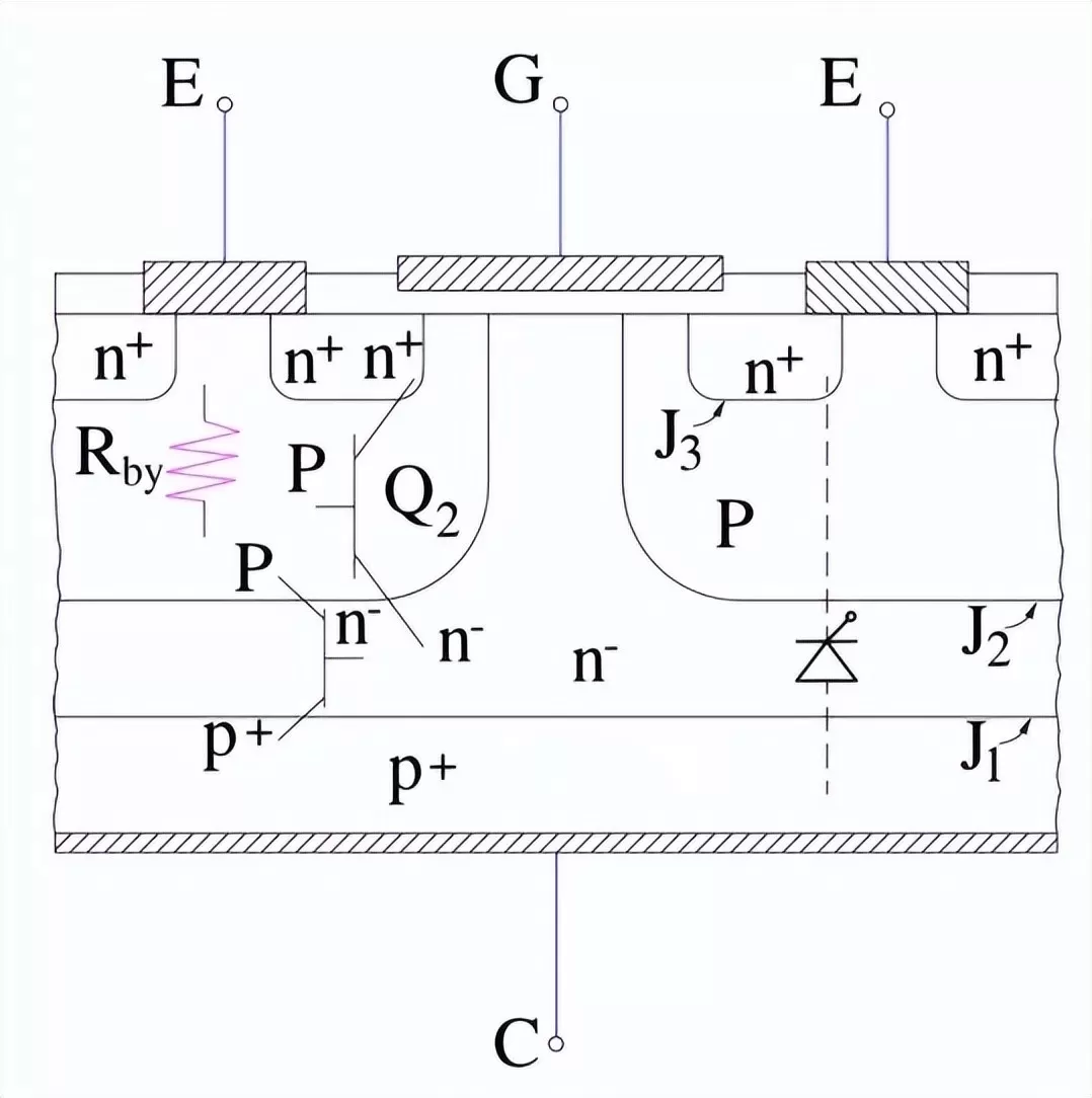
IGBTs have a metal layer attached to all three terminals (collector, emitter, and gate). However, the metal material on the gate terminal has a silicon dioxide layer.
The IGBT structure is a four-layer semiconductor device. The four-layer device is realized by combining PNP and NPN transistors, which form a PNPN arrangement.

As shown above, the layer closest to the collector region is the (p+) substrate, the injection region; above it is the N drift region, which includes the N-layer. The injection region injects most of the carriers (hole currents) from the (p+) into the N- layer.
The thickness of the drift region determines the voltage blocking capability of the IGBT. Above the drift region is the main body region, which consists of the (p) substrate near the emitter and, inside the main body region, the (n+) layer.
The junction between the injection region and the N-drift region is J2. Similarly, the junction between the N-region and the main body region is junction J1.
Note: The structure of an IGBT is topologically similar to a thyristor with a “MOS” gate. However, the thyristor action and function is suppressed, which means that only transistor action is permitted over the entire device operating range of the IGBT. IGBTs are preferable to thyristors, which wait for a fast switching over zero.
Working of IGBT
IGBTs operate by turning on or off by activating or deactivating their gate terminals. If a positive input voltage passes through the gate, the emitter hold drive circuit turns on. On the other hand, if the IGBT’s gate terminal voltage is zero or slightly negative, the circuit application is turned off. Since the IGBT can be used as both a BJT and a MOS tube, the amount of amplification it achieves is the ratio between its output signal and the control input signal.
For a conventional BJT, the amount of gain is roughly the same as the ratio of the output current to the input current, which we call and denote as β. On the other hand, for a MOS tube, there is no input current because the gate terminals are the isolation of the main channel carrying current. We determine the gain of the IGBT by dividing the change in output current by the change in input voltage.
An N-channel IGBT conducts when the collector is at a positive potential with respect to the emitter and the gate is also at a sufficiently positive potential (>V GET ) with respect to the emitter. This situation results in the formation of a reverse-type layer directly below the gate, which creates a channel, and current begins to flow from the collector to the emitter.
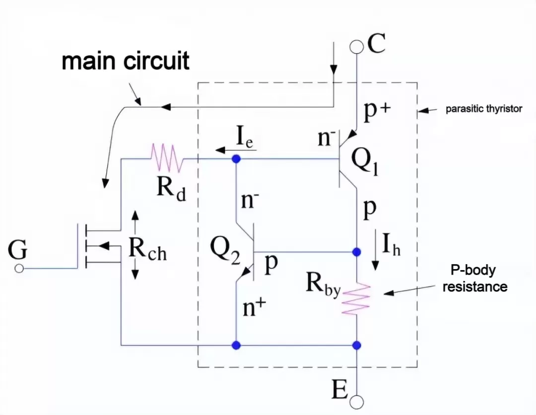
The collector current Ic in an IGBT consists of two components, Ie and Ih. Ie is the current that flows from the collector to the emitter due to the injected electrons through the injection layer, the drift layer, and eventually the channel, and Ih is the hole current that flows from the collector to the emitter through Q1 and the body resistance Rb. Thus although Ih is almost negligible, hence Ic ≈ Ie.
A special phenomenon is observed in IGBTs called IGBT latch-up. This occurs when the collector current exceeds a certain threshold (ICE). In this case, the parasitic thyristor is latched and the gate terminal loses control of the collector current, preventing the IGBT from turning off even if the gate potential drops below VGET.
To shut down the IGBT now, we need the typical current-switching circuitry, such as in the case of a thyristor forced current-switching. If the device is not shut down as soon as possible, it may be damaged.
Equivalent circuit of an IGBT
The approximate equivalent circuit of the IGBT consists of a MOS tube and a PNP transistor (Q1 ). Considering the resistance provided by the n- drift region, the resistor Rd is already included in the circuit, and this equivalent circuit can be derived by scrutinizing the basic structure of the IGBT, which is shown in the figure below.

Pass-through IGBT, PT-IGBT: Pass-through IGBT, PT-IGBT has N+ region at the emitter contact.
Observing the basic structure of the IGBT shown above, it can be seen that there exists another path from the collector to the emitter, which is the collector, p+, n-, p (n-channel), n+ and emitter.
Therefore, there is another transistor Q2 as n – pn+ in the IGBT structure, so we need to include this transistor Q2 in the approximate equivalent circuit to get the exact equivalent circuit.
The exact equivalent circuit of the IGBT is shown below:

Types of IGBT
IGBT can be divided into single IGBT, IPM (Intelligent Power Module), and other types of packages.
- Single IGBT: Single IGBT refers to a standalone IGBT device, usually provided in a discrete package. They are suitable for applications that require individual control and integration, and different packages and specifications can be chosen based on specific needs.
- IPM (Intelligent Power Module): IPM is a modular package that integrates multiple power electronic devices such as IGBTs, drive circuits, and protection circuits. IPMs typically contain one or more IGBT chips, drive circuits, and protection functions, simplifying design and improving system reliability. IPMs are widely used in motor drives, inverters, and other high-power applications.
In addition to single IGBT and IPM, there are other types of packages, such as:
- Digital IGBT: Digital IGBT is an IGBT package with integrated control and monitoring capabilities. They provide additional digital interfaces and functions to achieve advanced control and monitoring capabilities.
- Modular IGBT: Modular IGBT is typically a high-power IGBT module that integrates multiple IGBT chips, drive circuits, and heat dissipation systems. Modular IGBTs are suitable for high-power applications, such as large industrial drives and power conversion systems.
These different types of IGBT packages provide flexibility and diversity, allowing for the selection of the most suitable package type based on specific application requirements.
Characteristics of IGBTs
The fundamental attributes of an IGBT are its transfer and output characteristics.
Transmission Characteristics

IGBT transfer characteristics
The transfer characteristics of an IGBT, demonstrate the relationship between Ic and VGE. The transfer characteristics of IGBTs and MOSFETs share similarities. The flow of collector current necessitates a minimum threshold voltage, VTH, between the gate and emitter. The IGBT remains in the off-state when the gate-emitter potential is below the threshold voltage. Conversely, when the gate voltage exceeds the threshold voltage, the transfer curve displays linearity across a significant portion of the drain current.
IGBT output characteristics

IGBT output characteristics
Since IGBTs are voltage dependent, only a very small amount of voltage is required at the gate terminal to keep them on, as opposed to bipolar power transistors, which require a continuous base current flow in the base region to keep them saturated.
IGBTs are unidirectional devices, which means that they can only switch in the “forward” direction (from collector to emitter) IGBTs are the opposite of MOS tubes, which have a bi-directional current-switching process; MOS tubes are controllable in the forward direction, and the reverse voltage is not controlled. Under dynamic conditions, when the IGBT is turned off, it may experience latch-up current, which occurs when the continuous on-state drive current appears to exceed a critical value.
In addition, a small amount of leakage current flows through the IGBT when the gate-emitter voltage is below the threshold voltage, at which point the collector-emitter voltage is nearly equal to the supply voltage, and therefore the four-layer device IGBT operates in the cutoff region.
Advantages & Disadvantages of IGBT
IGBT as a whole has the advantages of both BJT and MOS tubes.
Advantages
- Higher voltage and current handling capability.
- Very high input impedance.
- Very high current can be switched using very low voltage.
- Voltage controlled device i.e. it has no input current and low input losses.
- Simple and inexpensive gate drive circuitry reduces gate drive requirements
- It can be easily turned on by applying a positive voltage and turned off by applying a zero or negative voltage.
- Has a very low on-resistance.
- Has a high current density, enabling it to have a smaller chip size.
- Has higher power gain than BJTs and MOS tubes.
- Has a higher switching speed than BJTs.
- High current level can be switched with low control voltage.
- Enhanced conductivity due to bipolar nature.
- Safer
Disadvantages
- Lower switching speed than MOS tubes.
- Unidirectional, cannot handle AC waveforms without additional circuitry.
- Cannot block higher reverse voltages.
- More expensive than BJTs and MOS tubes.
- Similar to the PNPN structure of thyristors, it suffers from latch-up problems.
- Longer turn-off time than PMOS tubes.
- PNPN structure similar to a thyristor with latching issues.
- Longer turn-off times than PMOS tubes.
IGBT Application
IGBTs are extensively employed in a diverse range of high-power applications.
- Motor drives: IGBTs are integral components in the regulation and control of electric motor speed across a wide range of industries, including automotive, aerospace, and consumer appliances. In the context of motor drives, IGBTs are employed in Voltage Source Inverters (VSIs) to convert a fixed DC voltage into an AC voltage with variable frequency and amplitude. This AC voltage is then utilized to govern the speed and torque of the motor. The high current handling capacity and rapid switching speeds of IGBTs facilitate efficient and precise motor control, thereby enhancing performance, energy efficiency, and reducing maintenance expenses.
- Power supplies: IGBTs are frequently employed in switching power supplies for high-voltage and high-current applications, including welding equipment, uninterruptible power supplies (UPS), and high-power DC-DC converters. The low on-state voltage drop and high switching speed of IGBTs are instrumental in enhancing efficiency and reducing heat dissipation in power supply systems.
- Renewable energy systems: In solar and wind power systems, inverters utilize Insulated Gate Bipolar Transistors (IGBTs) to convert the fluctuating DC power generated by solar panels or wind turbines into AC power. The use of IGBTs in these applications facilitates the swift and accurate regulation of voltage and current waveforms, which is crucial for the maintenance of maximum power point tracking (MPPT) and the achievement of efficient energy conversion.
- Electric vehicles: IGBTs are used in the traction inverters of electric vehicles (EVs), as these inverters are responsible for regulating the power that is supplied to the motors that propel the vehicle. The high voltage and current ratings of IGBTs enable them to effectively manage the high-power demands of electric vehicle propulsion systems. Additionally, their rapid switching speeds and minimal on-state voltage drop contribute to enhanced efficiency and decreased heat generation, which are critical factors in extending the driving range and battery life of electric vehicles.
- Power grid equipment: IGBTs are widespread in power grid equipment, particularly in High-Voltage Direct Current (HVDC) transmission systems and Flexible AC Transmission Systems (FACTS). In HVDC systems, IGBTs are employed in Voltage Source Converters (VSCs) to transform Alternating Current (AC) power into Direct Current (DC) power for efficient transmission over long distances. FACTS devices, such as Static Synchronous Compensators (STATCOMs) and Static VAR Compensators (SVCs), use IGBTs to regulate the flow of reactive power in the grid with high precision and speed. This results in improved power quality, stability, and reliability.
About GTAKE
GTAKE specializes in designing and producing innovative AC drives (also known as variable frequency drives), electric vehicle motor controllers, bidirectional DC sources, and test rigs with advanced control algorithms and cutting-edge technology, delivering optimal performance and reliability for industrial automation and new energy applications.
